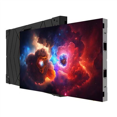
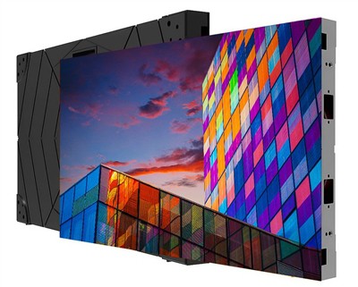
Many professionals exploring next-generation LED screens with ultra-fine pixel pitches quickly realize that microLED technology promises unmatched clarity and performance but faces steep hurdles on the factory floor. While traditional LED screens already deliver impressive large-format displays, scaling microLED to commercial volumes reveals just how complex turning microscopic emitters into reliable, affordable panels actually becomes.
At its heart, microLED manufacturing involves growing tiny inorganic LEDs - often smaller than 100 micrometers - and then precisely placing tens of millions of them onto a display backplane for each panel. For a 4K display, that can mean handling around 25 million pixels or roughly 75 million individual RGB sub-pixels. The core process, known as mass transfer, requires moving these chips with sub-micron accuracy at extremely high speeds to keep production economical. Current techniques often fall short, with placement needing to happen in minutes rather than hours or days for viable throughput.
Yield stands out as one of the biggest practical headaches. Even a seemingly strong 99.99% success rate leaves thousands of defective pixels on a high-resolution panel, forcing expensive and time-consuming repair steps that can add hundreds of dollars per unit. Industry targets aim for 99.9999% or better - six nines - to minimize intervention, yet many pilot lines hover closer to 99.98–99.99%. Defects arise from multiple stages: epitaxial growth on wafers, chip singulation, transfer itself, and bonding to the backplane. Red LEDs prove especially tricky, as efficiency drops sharply at very small sizes, complicating full-color architectures that often rely on different materials for red, green, and blue.
Cost structures reflect these difficulties. Die fabrication and mass transfer equipment demand heavy capital investment, while material constraints around substrates like gallium nitride add supply chain pressure. Without standardization, manufacturers develop custom processes and tools, inflating non-recurring engineering expenses. For large LED screens aiming at fine pitches below 1 mm, these factors push production costs far above those of conventional LED or LCD alternatives, sometimes by several times, limiting microLED today mostly to premium or niche applications rather than broad commercial rollout.
Other real-world factors compound the challenge. Achieving consistent brightness and color uniformity across massive arrays requires flawless integration with driving electronics. Heat management, testing protocols, and scaling wafer sizes all play roles, and shifts in pixel pitch toward the sub-1 mm range amplify every precision demand. Some approaches explore monolithic RGB designs or alternative transfer methods like laser-based or fluidic assembly to improve speed and yield, but each brings its own trade-offs in equipment complexity and process maturity.
From countless development efforts, the pattern is clear: finer pixel pitches in microLED unlock closer viewing distances and higher perceived resolution on compact or seamless walls, yet they intensify manufacturing demands. Overlooking these realities leads to mismatched expectations on timelines and budgets for projects targeting control rooms, high-end signage, or dynamic events.
In the end, overcoming microLED manufacturing challenges will determine how quickly ultra-fine pitch LED screens move from high-end prototypes to widespread, cost-effective solutions. Progress in yield optimization, standardized processes, and efficient mass transfer continues to build momentum, gradually expanding viable applications across premium displays, automotive, and large-scale visual experiences where superior brightness, contrast, and longevity outweigh current hurdles. As these barriers ease, microLED stands poised to redefine performance benchmarks in the evolving LED display landscape.